
In this guide, we’ll walk you through practical steps to integrate GLGNET SFP connectors and QSFP into your PCB, helping you avoid common design mistakes and ensure stable, high-speed operation.
If you’re also facing compatibility concerns when using mixed-brand transceivers, check out our article on How to Fix SFP Connectors' Brand Compatibility Issues for practical solutions.
https://www.glgnet.biz/articledetail/how-to-fix-sfp-connectors-brand-compatibility-issues.html
SFP connector types
|
Application |
Recommended GLGNET Connector |
|
Single-port, low-speed design |
1-piece or 2-piece SFP |
|
Multi-port compact layout |
Ganged 1x2, 1x4, 1x6 SFP |
|
High-density stacked design |
Stacked 2x1 to 2x8 SFP |
|
10G to 40G data transmission |
QSFP with EMI & Heat Sink options |
|
High faceplate port density |
QSFP Low Insertion Force models |
Choosing the appropriate SFP connector is a key factor in achieving reliable performance and ensuring long-term stability in your PCB design. GLGNET offers a diverse portfolio of SFP solutions, designed to meet a wide range of application needs—from standard networking equipment to space-constrained, high-density systems.
● Single-Port SFP (GLGNET 1-piece & 2-piece models)
Ideal for designs requiring a small number of ports, these connectors offer a simple, robust solution without sacrificing mechanical stability.
GLGNET provides both DIP and press-fit mounting options, giving engineers flexibility to align with different manufacturing processes. To support system-level visibility, optional light pipes can be integrated for status indication. For applications with higher power or thermal demands, heatsink options are also available to help maintain optimal operating temperatures.
● Ganged SFP (GLGNET 1x2, 1x4, 1x6 configurations)
When board space is at a premium but higher port density is required, GLGNET’s ganged SFP configurations deliver a compact, efficient solution.
By combining multiple ports into a single, streamlined assembly, these connectors help maximize available space while maintaining reliable electrical performance. Ganged SFPs use a standard 20-pin SMT footprint and can be equipped with optional light pipes for visual feedback, as well as heatsinks to enhance cooling and system stability in demanding environments.
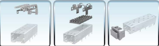
● Stacked SFP (GLGNET 2x1, 2x2, 2x4, 2x6, 2x8 configurations)
For designs focused on maximizing port count within minimal PCB area, stacked SFP assemblies are the optimal choice.
These SFP module connectors feature a vertical port arrangement, significantly increasing connectivity without expanding the board footprint. GLGNET’s stacked SFP module connectors are also available with light pipe options, ensuring clear, real-time status indication even in the most densely populated layouts.
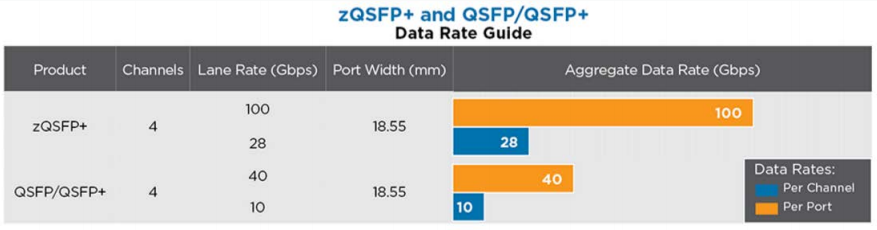
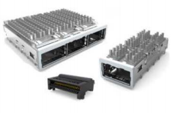
For applications demanding higher bandwidth, GLGNET’s QSFP series offers a reliable solution for data rates of 40Gbps and beyond. These connectors utilize a standardized 38-pin interface, ensuring seamless integration with most system designs. Compared to conventional SFP connectors, QSFP provides up to three times the port density, and four times the density of older XFP solutions, making them ideal for space-constrained, high-performance environments.
To meet diverse design requirements, GLGNET QSFP connectors are available with multiple options, including integrated heatsinks for thermal management, light pipes for visual status indication, and EMI shielding cages for enhanced signal integrity. Designers can choose between through-bezel or behind-bezel mounting styles, providing flexibility based on the product’s mechanical constraints. For ultra-dense faceplate layouts, low insertion force versions are also available, simplifying assembly and reducing mechanical stress during module installation.
Thoughtful placement of SFP and QSFP connectors is fundamental to ensuring reliable system performance, straightforward assembly, and long-term product durability. From both a mechanical and functional perspective, positioning these connectors along the PCB edge—ideally in line with the enclosure’s front panel—is considered best practice. This arrangement simplifies module insertion and removal while minimizing the risk of mechanical strain on the board during operation.
Beyond basic positioning, it is essential to allocate sufficient clearance around each connector footprint. This includes not only space for cable access and latch operation but also room for critical accessories such as heatsinks, EMI cages, and light pipes. In high-density designs, overlooking these spatial considerations can result in cable interference, obstructed airflow, or difficulties during assembly and future maintenance.
Moreover, designers should account for the full mechanical profile of both the connector and the transceiver module, considering factors like insertion depth and module retention features. Leveraging accurate 3D models from trusted suppliers such as GLGNET during the PCB design phase is highly recommended. This approach helps validate fitment within the final product housing, ensures proper alignment with panel cutouts, and reduces the likelihood of costly rework or mechanical failure in production.
In high-speed or compact system designs, where every millimeter counts, careful placement and clearance planning are not optional—they directly impact signal integrity, thermal management, and the overall user experience.
Effective signal routing is a critical factor in ensuring stable performance when integrating SFP or QSFP connectors, especially in applications involving high-speed data transmission. Poor routing can quickly compromise signal integrity, leading to reduced system reliability.
To optimize performance, differential pairs connecting to the connector SFP should be routed as short and direct as possible. Keeping trace lengths minimal helps reduce signal attenuation and lowers the risk of external noise coupling into the signal path.
Precise length matching between the two traces of each differential pair is equally important. Even small mismatches can introduce timing skew, which is detrimental to maintaining clean, high-speed signal transmission. Targeting a differential impedance of 100Ω along the entire routing path is recommended to prevent reflections, impedance mismatches, and overall signal degradation.
Where feasible, the number of vias along high-speed differential traces should be kept to a minimum. Each via introduces impedance discontinuities and can negatively affect signal quality, particularly in multi-layer PCB designs. If vias cannot be avoided, carefully controlling their geometry is essential to maintaining consistent electrical performance.
Additionally, high-speed differential pairs should always be routed over a continuous ground plane. An uninterrupted ground reference not only stabilizes impedance but also helps minimize electromagnetic interference (EMI) and ensures clean, low-noise return paths for the signals.
By applying these best practices, PCB designers can significantly improve signal integrity, reduce EMI exposure, and enhance the overall reliability of connector SFP in high-speed circuit layouts.
A robust grounding layout is essential to ensure consistent electrical performance when integrating SFP female connectors into your PCB design. For best results, maintain a continuous ground plane directly beneath the SFP or QSFP footprint. This provides a stable reference for high-speed differential signals and helps minimize impedance fluctuations that could compromise signal integrity.
To further strengthen the ground network, incorporate stitching vias around the connector area, especially near the attachment points for EMI cages or shielding components. These vias create low-impedance connections between PCB ground layers, improving signal return paths and helping to control electromagnetic interference (EMI).
On the power side, pay close attention to decoupling. Place decoupling capacitors as close as possible to the power supply pins of the SFP female connector to suppress voltage ripple and reduce noise. This step is particularly important for higher-speed applications, such as SFP+ and QSFP modules, which demand stricter power integrity and stable voltage rails to operate reliably.
Following the precise footprint recommendations from your SFP connector manufacturer—such as GLGNET—is critical to achieving reliable mechanical alignment and long-term product durability. Small deviations in pad placement, drill tolerances, or hole sizes can lead to soldering defects, mechanical stress, or difficulties during module installation.
In high-speed designs, especially those using SFP+ or QSFP modules, thermal management becomes an equally important consideration. Adding copper pours around the connector footprint helps dissipate heat, while placing thermal vias within these copper regions allows for efficient heat transfer to internal PCB layers or external cooling solutions.
For designs with multiple stacked or ganged SFP connectors, maintaining adequate airflow around the connectors is essential. Ensuring proper ventilation not only improves heat dissipation but also contributes to the overall stability and service life of both the connector and the transceiver module.
Before completing assembly, thorough inspection and testing are necessary to confirm reliable SFP module connector integration. Start by visually checking solder joints for uniformity, proper wetting, and correct alignment—especially for connectors with a high pin count or press-fit configurations.
Real-world functional testing should also be conducted using actual SFP or QSFP modules to verify proper insertion, secure locking, and ease of removal. This helps detect any mechanical interference or fitment issues that may have been overlooked during the design phase.
For electrical verification, utilize diagnostic tools such as Time-Domain Reflectometers (TDR) or oscilloscopes to evaluate impedance consistency, check for signal reflections, and assess overall signal integrity across the high-speed differential pairs. Identifying and resolving signal quality issues early helps prevent more significant performance problems later in the product lifecycle.
Learn more:
https://www.glgnet.biz/articledetail/what-type-of-sfp-fiber-connector-should-you-choose
https://www.glgnet.biz/articledetail/how-sfp-connectors-boost-data-center-performance
https://www.glgnet.biz/articledetail/why-is-my-sfp-port-not-working-common-issues-and-fixes
Conclusion
A well-executed SFP connector layout requires more than just choosing the right component—it demands careful attention to placement, signal integrity, grounding, thermal management, and thorough validation.